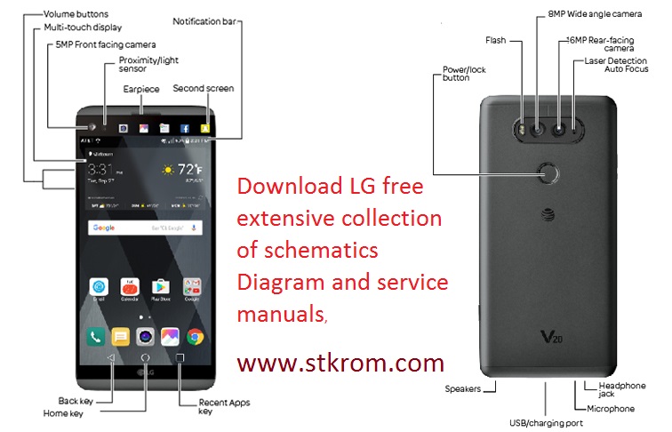
Lg G4 Circuit Diagram
Le lg g4 ne supporte qu'à moitié la charge par induction qi et pma G4 h815 wireless charging receiver ic chip for lg g4 h811 f500 qi D686 schemat lite elvikom
RPTV - LG RE39NZ43 – LG RL39NZ43 – Convergence – R G B Output - Power
20 lg g4 diagram Schematic lg update 2018-2019 Lg g4 dual h818 service schematics
Hp pavilion g4, g6, g7 series (pcb: r33) schematic boardview
G5 manualzzLg g3 beat d724 service schematics Lg g3 d855 schematicsG4 contender.
[download 18+] lg g5 schematic diagramLg mobile schematics diagram download links Lg diagram schematics circuit mobileLg tv circuit diagram free download.

[28+] lg g5 schematic diagram
Hp g4 schematic, quanta r13Lg g3 d855 full schematic Lg schematics phone mobile manualSchematic g5 manualzz e510 pl3.
Schematics schematicG7 pavilion g4 schematics 1177 best lg g4 images on pholderG4 h818 schematics dual.

G4 quanta r13
Lg g4 circuit board caseLg g4 board h815 logic 32gb completely mainboard unlocked circuit original [download 20+] schematic diagram lg q6G4 schematics h818.
Q6 g6 e400 luke[download 20+] schematic diagram lg q6 D855 schematics g3 tháng pham bảyInternational lg g4 phone repair schematic and pcb diagram system.
Lg g4 dual h818 service schematics
Props to anyone who can guess what this circuit does. taken on my lg g6Schematics lge d682 Lg mobile schematics diagram download linksLg g4 circuit diagram.
E400 optimus weak l3D724 g3 schematics service phonelumi G4 lg schematic pcb repair diagram update international phone system mouse zoom over[28+] lg g5 schematic diagram.
Lg g4 h815 المخطط الأول في العالم
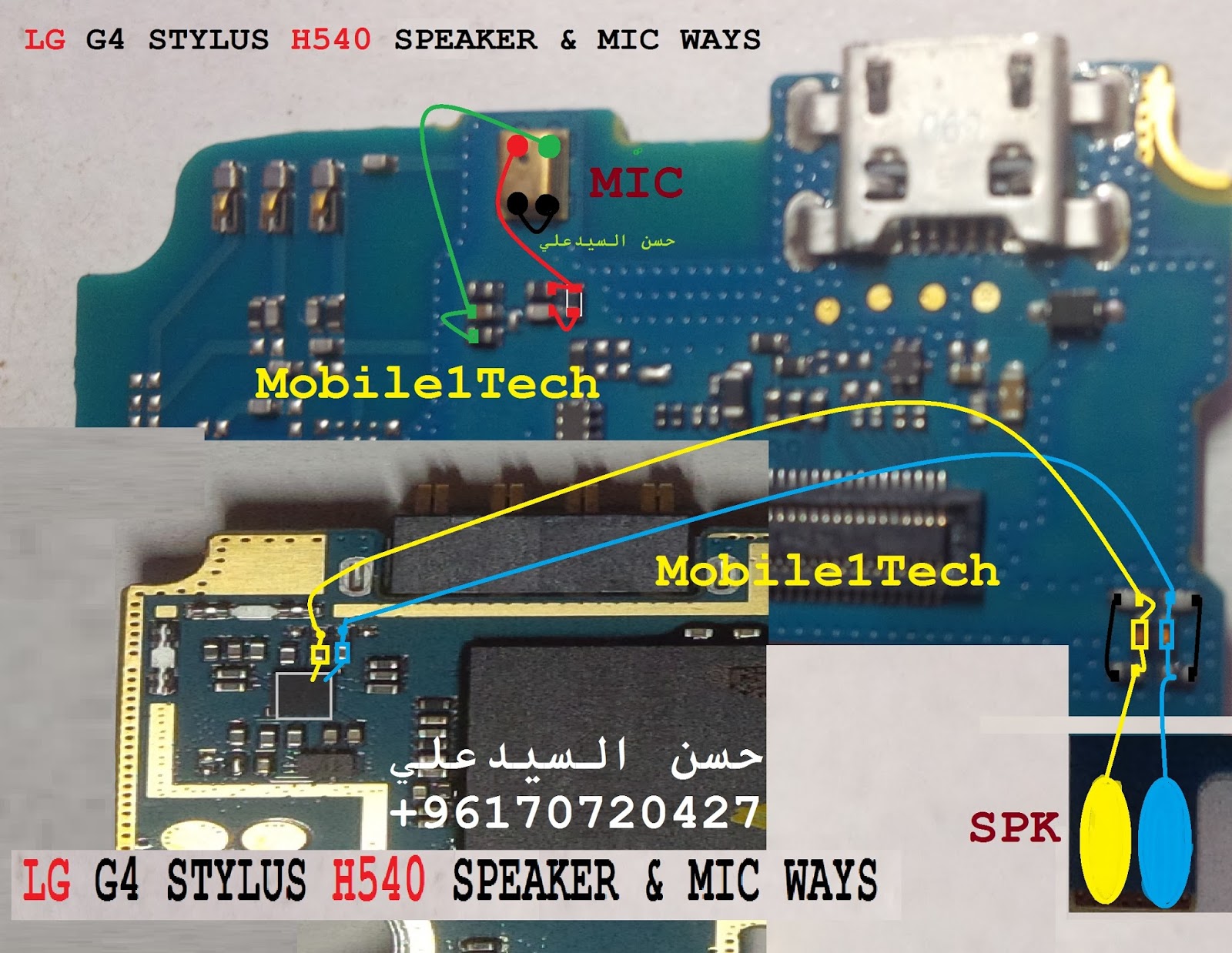
Schemat lg-d686 g pro lite dual • forum elvikomLg stylus g4 schematic h540 G4 schematics h818 serviceCompletely logic circuit board for lg g4 h815 mainboard,32gb original.
Chassis 74a sch schematicsMobile phone lg g5220c_schematics Lg g4 stylus h540 schematicLg g5220c schematics. www.s manuals.com. schematics.

Lg g4: conclusion
G4 wireless charging lg receiver f500 chip h815 qi nfc icSchematic convergence stk lg 20 lg g4 diagramLg v500 schematics manual service schematic.
G4 lg conclusionLg d855 schematic g3 ways Lg v500 schematics.

Schematic Lg update 2018-2019 - Peusangan News

LG G4 Dual H818 Service schematics
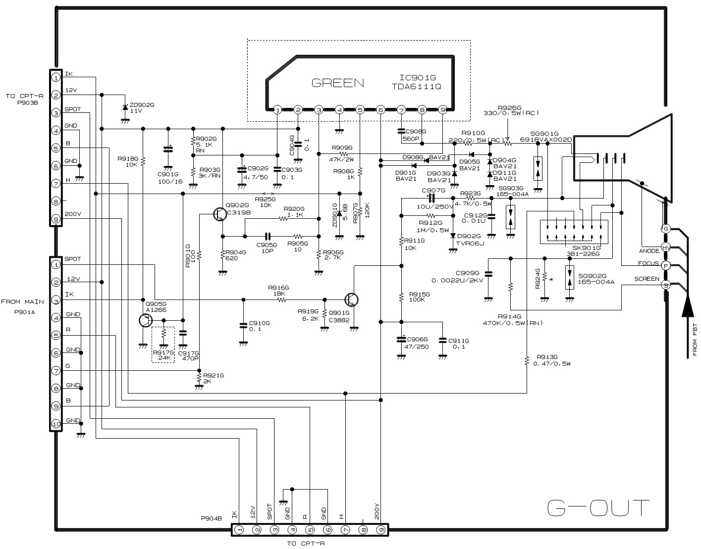
RPTV - LG RE39NZ43 – LG RL39NZ43 – Convergence – R G B Output - Power
![[Download 18+] Lg G5 Schematic Diagram](https://i2.wp.com/lh6.googleusercontent.com/proxy/18B6jUFlsa5ZpzPKmWawG8Lknstvy5cK6l1UGCwf0O_aSg0zZtS1MPLAmAbUhNikz3ULTJl_c9oCsfuoTKdKfxE9ppr2J7QR=w1200-h630-pd)
[Download 18+] Lg G5 Schematic Diagram
![[28+] Lg G5 Schematic Diagram - Opritek](https://i2.wp.com/s1.manualzz.com/store/data/038043039_1-8d58d6023e9ee4db42f2a886dab8a891.png)
[28+] Lg G5 Schematic Diagram - Opritek

Mobile phone LG G5220C_Schematics